For accurate microchip encapsulation paddle-shift analysis, cross flow through the leadframe openings must be considered.
Paddle shift is caused by the pressure difference between the upper and lower cavities of the leadframe. To calculate the pressure difference accurately you need to model cross flow.
For a typical QFP chip, openings in the leadframe exist at the corner, side and periphery of the chip, as shown in Figure 1 below. In modeling the openings for Fill+Pack analysis using the Hele-Shaw approximation, we need to consider the juncture loss associated with the flow across the openings. Because of the juncture loss, the modeled openings will not be the same size as the actual openings. To calculate the size (thickness) of the opening to be used in the model, use the equations below.
where
and
 when
when 
 when
when 
 when
when 
where:
-
 is
is  ,
, -
 is the power-law index,
 -
 is half of the opening width,
 -
 is half of the distance between the solid region,
 -
 is half of the opening width to be used in the model.
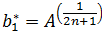
The length of the opening in the model can be used as the thickness of the leadframe. For the periphery around the chip (as shown in Figure 1 below), can be assumed to be half of and  is the thickness of the leadframe. When =0.74,
  = 1.2041,
  = 0.2501 and
  =0.903. The values of , and only slightly depend on , so these values can be used for other values of . For approximation,
  can be taken as
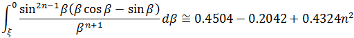
  . The integral term in equation 2 can be approximated by :
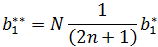
In some regions there are too many openings to be modeled in the simulation. For example, there may be tens of openings in the side region. The following equation can be used to combine  openings of the same size into one, and to determine the size of the single opening:
Regarding the thickness of the cavity, we can use the thickness of one side for modeling. However, for a large opening (at periphery of the chip), use the combined thickness of two cavities. In the model, wires can be neglected.
Another way to model the cavity is as follows. The thickness of the large opening region at the periphery of the chip is modeled as that of one side of the cavity. However, the shape factor of this region is 0.5. Other regions have a shape factor of 1.
An example of a chip cavity model is shown in Figure 1. In this model, there are upper and lower cavities, and cavities that connect the upper and the lower cavity. The upper and lower cavity is separated by L (the thickness of the leadframe).

One example of cavity modeling with cross-flow elements
where:
-
 = upper cavity
 -
 = cross-flow elements
 -
 = lower cavity