When you set up your CFD simulation from a CAD model, various part and assembly geometry issues can negatively impact the mesh completion or mesh quality. For assemblies, the MAT assesses three geometry situations and provides you with the resulting data and settings to aid your investigation. Use the MAT and your engineering judgment to determine the importance of potential issues and plan for any needed remedies. Once you find issues, return to your CAD application and modify the geometry appropriately.
Model Slivers
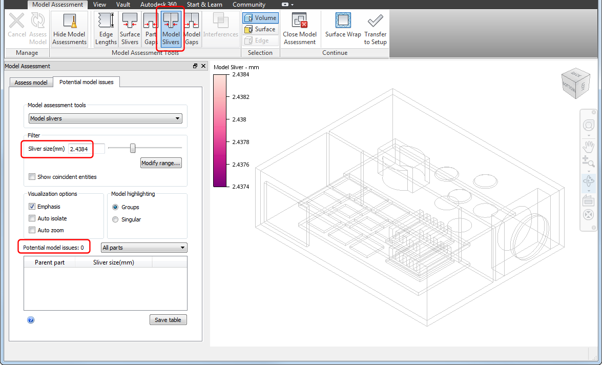
Assembly parts can interface such that surfaces with large aspect ratios, also known as sliver surfaces, are created. Sliver surfaces require fine mesh seeding which can significantly increase mesh counts. Sliver surfaces can also introduce local discontinuous behavior in the mesh length scales which negatively impacts solution accuracy. Use the Model Slivers tool to assess your model for potential sliver surface issues.
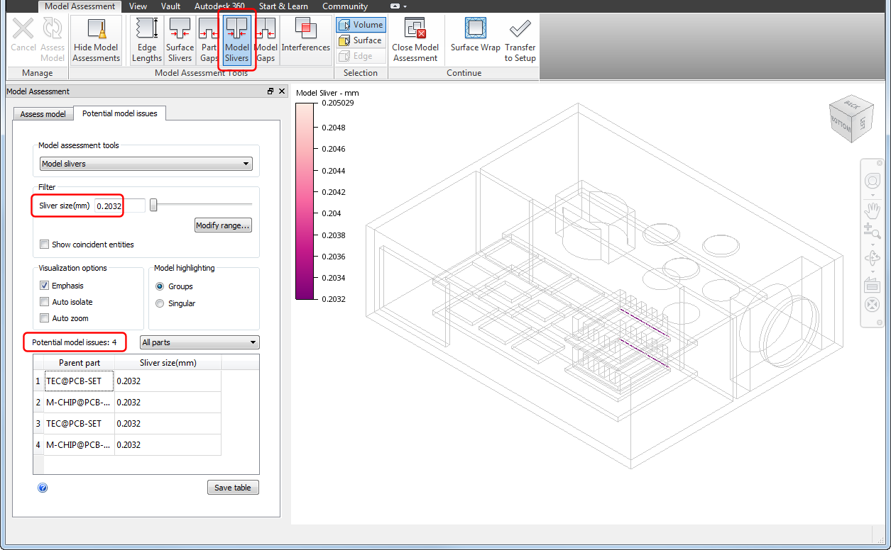
The following image shows our electronics enclosure assembly model with the Model Slivers tool active. The initial sliver size filter setting defaults to 0.2032 mm, resulting in 4 potential sliver issues.
When you select the table entries and Auto zoom and Emphasis, you see the potential sliver issues at the interfaces of the chips and heat sinks.
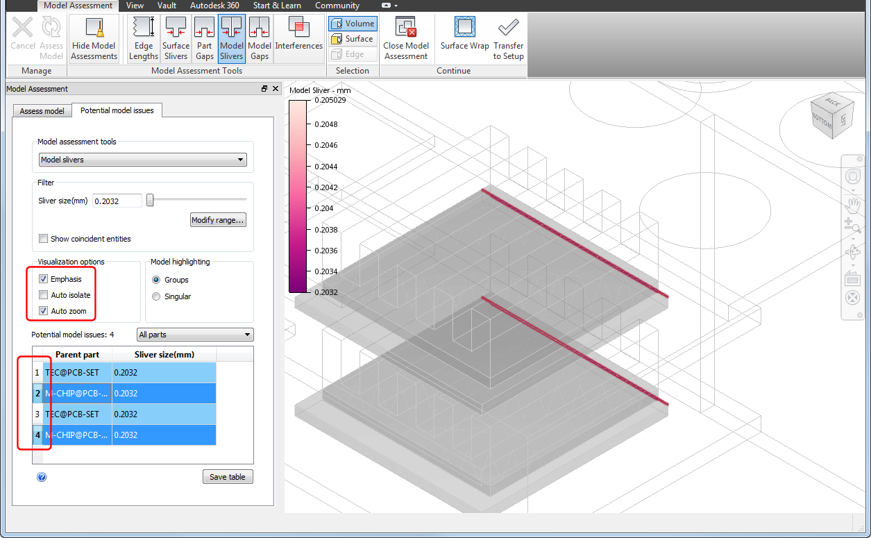
By rotating and zooming the view, we see a small offset between the edges of the heat sinks and chips. If you transferred this model into CFD in the current configuration, these offset edges would result in the creation of small sliver surfaces.
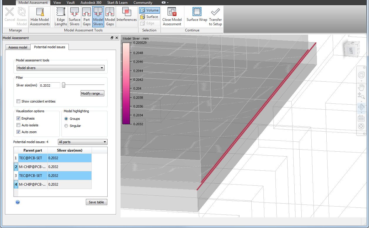
Most likely, this small offset is the result of improper applications of assembly constraints. As a result, we can return to Inventor and apply the proper constraints to eliminate the small offset at the interfaces.
Model Gaps
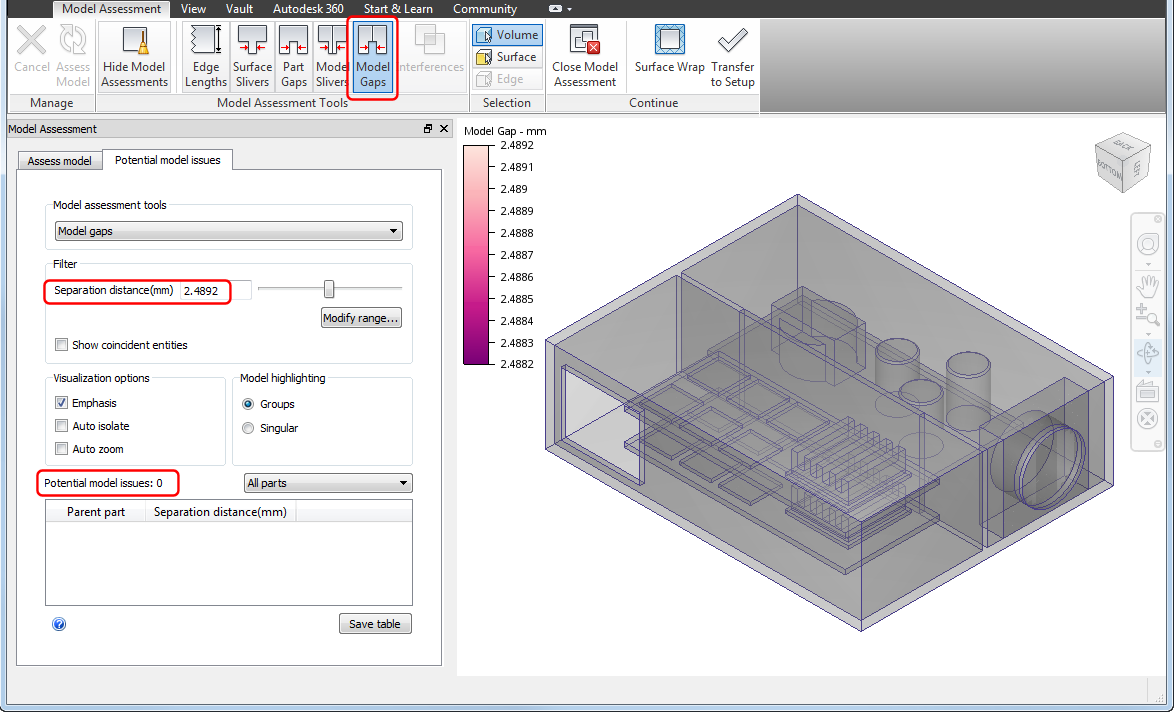
Similar to model slivers, small gaps between assembly parts can also result in mesh length scale issues. Use the Model Gaps tool to assess your model for small gaps that may challenge the CFD mesher.
Returning to our model and using the Model Gaps tool, the initial filter size setting defaults to 0.127 mm resulting in 4 potential gap issues.
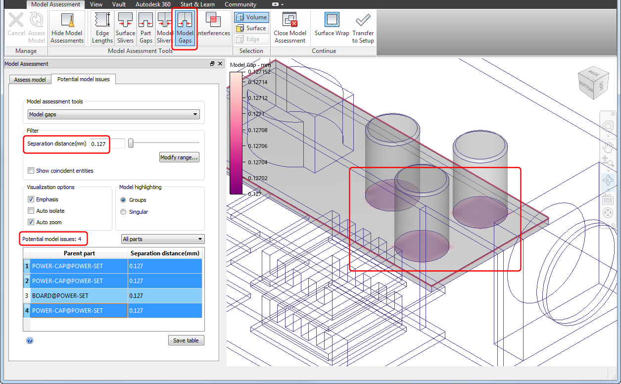
Rotating and zooming the view, we see small gaps between the capacitors and board.
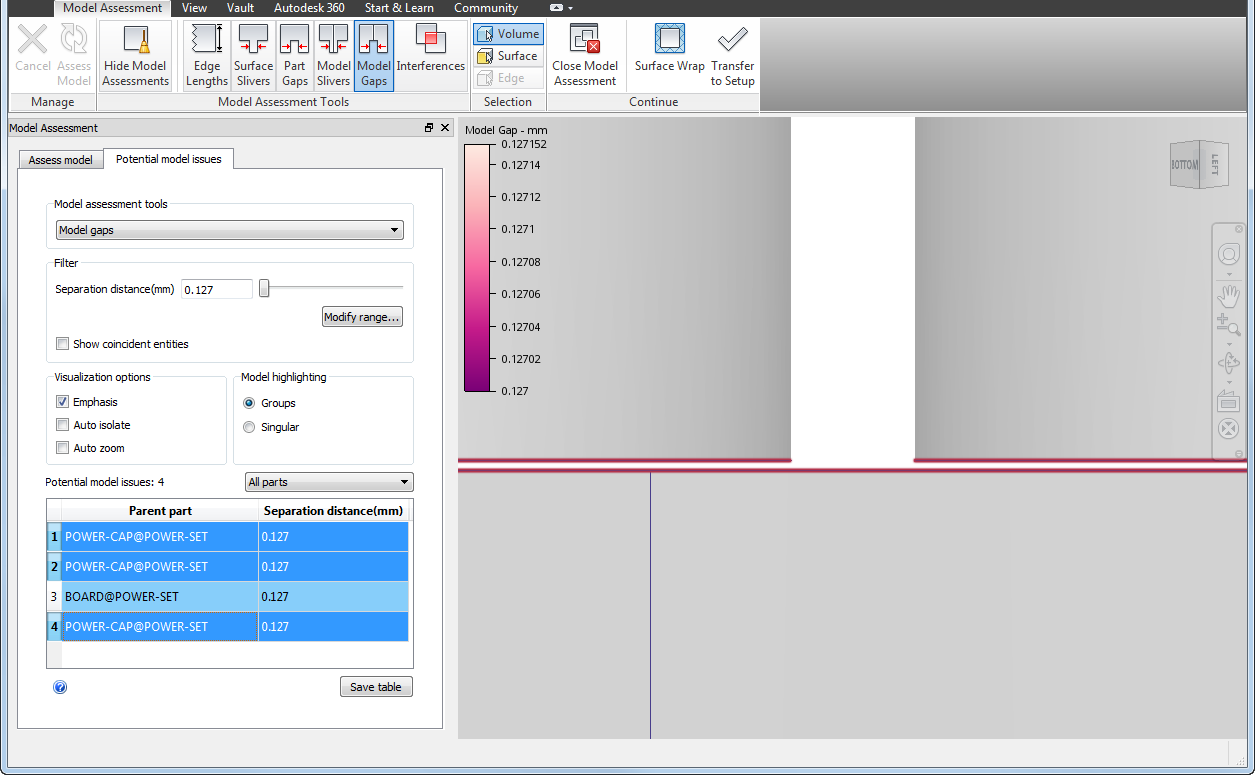
Clearly, these gaps are not reflective of our physical design and should be eliminated before the model is transferred to CFD. Therefore, we return to Inventor and apply proper constraints to eliminate the gaps between the capacitors and board.
Interferences
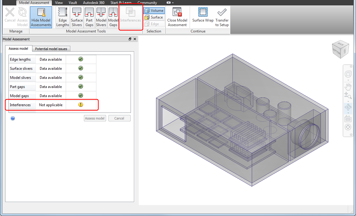
If interferences result, due to interfacing parts, unexpected results can occur when transferring your model to CFD. You can end up with additional fluid or solid parts in your simulation model due to the Boolean operations involved. These parts can impact your setup and meshing operations leading to process inefficiencies, meshing errors, and modeling inaccuracies.
Returning to our electronics enclosure assembly model and using the Interferences tool, we find 12 interference issues between the chips and boards.
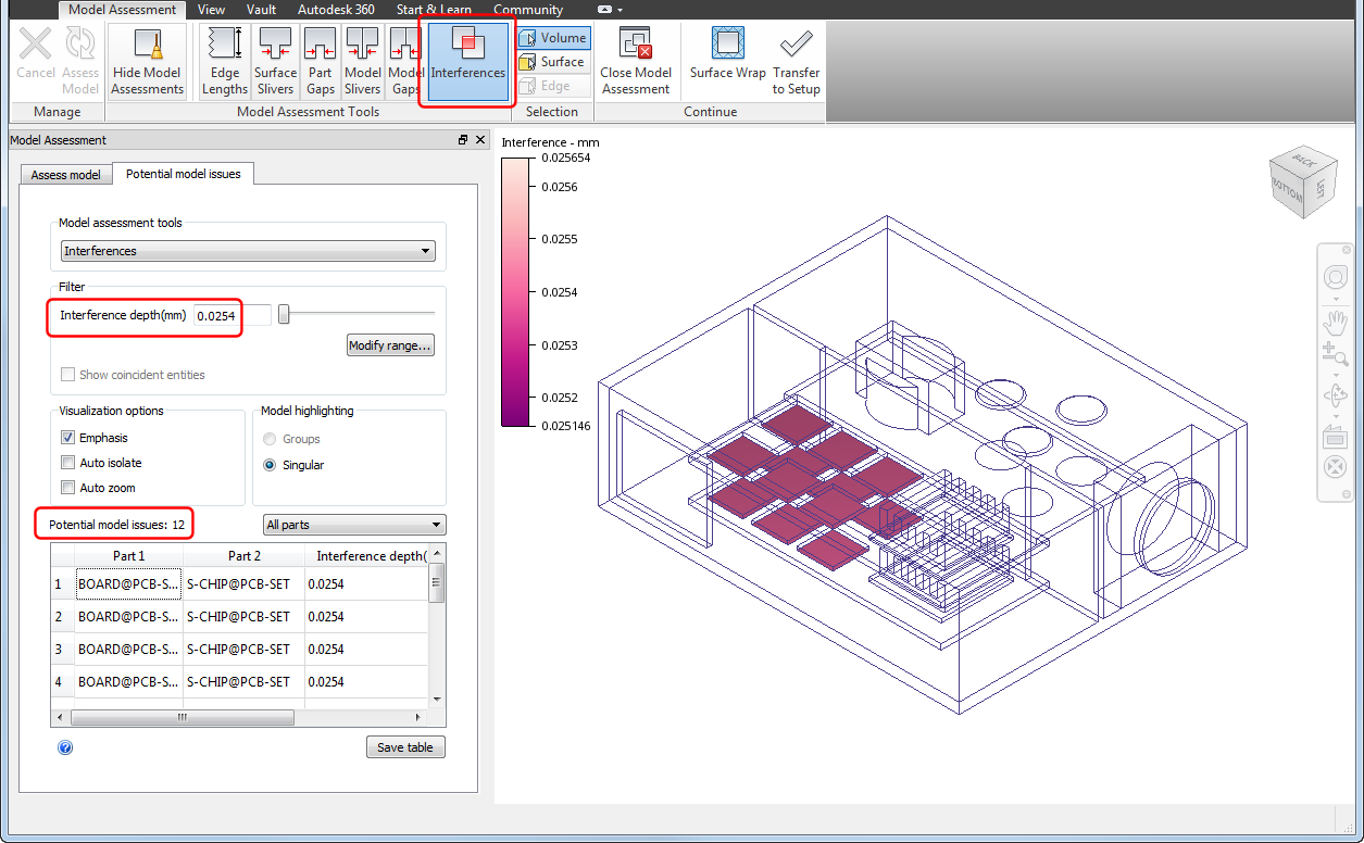
When we rotate and zoom the view, we see interferences occur where the leading edges of the chips extend below the board surface.
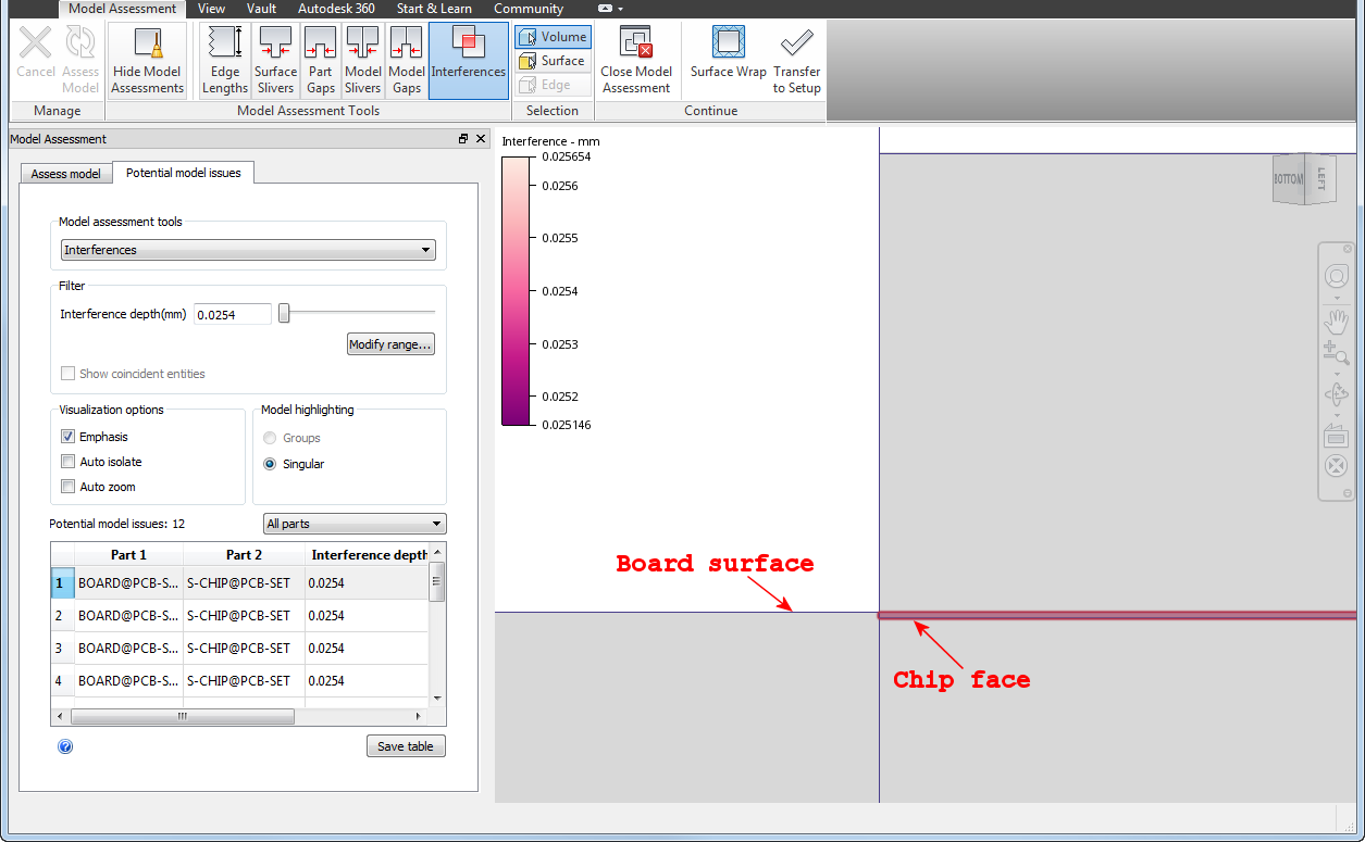
If an interference is small enough, it can be within the CFD modeling tolerances and eliminated during the meshing process. However, if the interference is larger than the modeling tolerances, you can end up with significant issues.
We transferred the model into CFD with the existing interference conditions. The following image shows one of the printed circuit board (PCB) assemblies. We know that interferences exist between the chips and the board, but the image doesn't show any obvious issues.
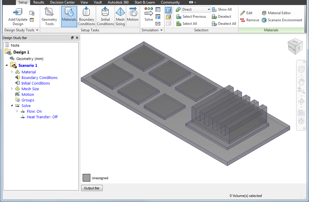
In the next image, we select all six of the chips. Again, nothing looks amiss.
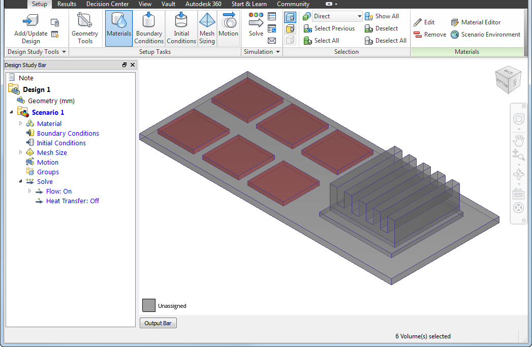
However, once we hide the chips, we see an interesting result. The following image shows that the interferences between the chips and the board were converted into additional chips. We now have 12 chips per PCB assembly - six thin chips embedded into the board and six chips on top of those embedded chips.
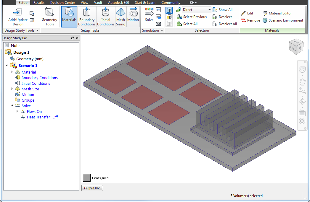
Clearly, this chip configuration no longer represents our physical design. As a result, we need to return to Inventor and eliminate the interferences so that we end up with only six chips mounted to the board.
Reworked Assembly
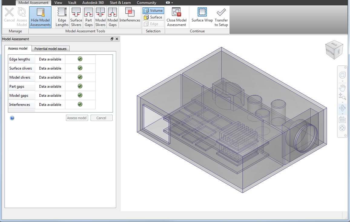
Upon returning to Inventor, we updated our assembly constraints to ensure that:
- the heat sinks are centered on the chips,
- the capacitors contact the board,
- the chips contact the boards without interference.
