Create the Circuit Builder circuit template drawing, an AutoCAD .dwg file that contains the wiring framework for the circuit.
Copy Similar Existing Circuit Template
- Locate the existing circuit template drawing file ace_cb1_FVNR_H.dwg. Copies of the circuit builder templates are installed in each of the schematic library folders, JIC125, IEC2, and so onto. Copy this file to ace_cb1_FVNR_H_custom.dwg. Note: The circuit template name is not critical and does not affect functionality of Circuit Builder.
- Open the copied and renamed circuit template, ace_cb1_FVNR_H_custom.dwg, in AutoCAD. Make sure that you have write access to the drawing.
This template consists of three wires and some marker blocks.
- Open ace_circuit_builder.xls in a spreadsheet software for reference. See Circuit Builder spreadsheet overview for the location of this file.
Use standard AutoCAD commands to modify the template and not AutoCAD Electrical toolset commands. It avoids creating a template that contains an extra copy of the AutoCAD Electrical toolset WD_M block. If you accidentally use a command that inserts the invisible WD_M block, either UNDO or erase and purge the WD_M block instance. To erase and purge the invisible block, follow these steps:
- Enter ATTDISP at the command prompt.
- Enter ON to make all attributes visible.
- Locate the block at 0,0.
-
Click
 .
.
- Select the block and press enter.
- Enter PURGE at the command prompt.
- Select WD_M in the Block s section.
- Click Purge.
- Click Close.
Define wires stretching to connect to bus
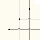
The first modification is to change the way the horizontal wires connect to the vertical bus when inserted. The copied template is defined as follows:
- Top wire skips over two wires and connects to the left-most vertical bus wire.
- Middle wire skips over one wire and connects to the middle vertical bus wire.
- Bottom wire connects to the first vertical bus wire it encounters.
The following changes to the marker blocks reverse it.
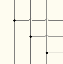
- Zoom in on the left-hand side of the template.
You should see three marker blocks, each with a CODE value of WCON. Each one is directly on top of and near the end of one of the wires.
- Enter ATTEDIT and select the top WCON marker block.
You should see the following values:
- CODE = WCON - maps back to a row in the circuit codes sheet with a function to stretch the end of the underlying wire to try to make a connection.
- ORDER = 1.02 - indicates the order of processing for the marker block relative to all the other marker blocks in the template. The order value can be an integer number or a decimal number. The blocks are processed low to high starting at 0. Blocks with the same ORDER value are processed as a group.
- MISC1 = _WIRESKIP=2;_MAXTRAPCOUNT=200 - defines any special handling of the marker block. See the Marker block attributes topic for a complete list of supported values.
- Change the MISC1 value to _MAXTRAPCOUNT=200, removing _WIRESKIP=2.
The _WIRESKIP value defines the number of wires to skip over when trying to connect to the vertical bus when inserted. Removing this value directs Circuit Builder to connect to the first vertical wire it finds.
The _MAXTRAPCOUNT limits the relative distance that circuit builder searches to find a wire to connect to. It is measured in an integer number of wire connection trap distance units. If _MAXTRAPCOUNT is not defined or is zero, the search is across the whole extents of the drawing.
- Click OK.
- Enter ATTEDIT and select the bottom WCON marker block.
- Change the MISC1 value to _WIRESKIP=2;_MAXTRAPCOUNT=200, making sure to enter the semi-colon character between the values.
It tells Circuit Builder to skip over two vertical wires when trying to connect to the vertical bus and to search up to 200 times the trap distance for a vertical wire to connect to. If none are found within that distance, Circuit Builder will not stretch this wire.
- Click OK.
Remove unnecessary marker blocks
The copied circuit has marker blocks for a control transformer and power factor correction capacitor. For this custom circuit, these options are not needed and the marker blocks can be removed.
- To verify which marker block is for the control transformer, switch over to ace_circuit_builder.xls.
- Open the ACE_CIRCS worksheet.
Find which circuit codes sheet is used for the original template you copied over, ace_cb1_FVNR_H.dwg.
- Locate a row with the name of the original template you copied over, ace_cb1_FVNR_H.dwg, in the DWG_TEMPLATE field.
- Find the SHEET_NAME value for this row, 3ph_H.
- Open the 3ph_H worksheet.
- Find the entry for Control transformer and circuit - non-reversing in the COMMENTS column.
- Find the CODE value for this row, XF01.
This CODE value links the marker block to the circuit code sheet.
- Switch back to the drawing and locate the marker block with the CODE value of XF01.
- Erase the marker block using the AutoCAD ERASE command.
- Repeat the steps to locate and delete the power factor correction marker block, CODE=KVAR1.
Add a marker block
You can add a marker block by inserting the library symbol, ace_cb_marker_block.dwg, or by copying an existing marker block and modifying the attribute values. In this section, you will insert a marker block that directs Circuit Builder to display a list of possible components to insert in the Circuit Configuration dialog box.
- Determine exactly where in the template you want this specific component inserted as the circuit is built.
- Enter INSERT at the command line to launch the AutoCAD block insert command.
- Browse to ace_cb_marker_block.dwg and insert this block at the desired location.
A copy of this block is installed in each of the schematic library folders, JIC125, IEC2, and so on.
Note: You could also use the AutoCAD COPY command and copy a nearby marker block into the desired location. - Enter ATTEDIT and select the marker block.
- Enter a value for the CODE attribute, for example USR001.
Use letters or numbers for the value. There is no code naming convention. Make sure it is unique within the circuit codes spreadsheet. This marker block code value maps a row or group of rows in to the spreadsheet. The information in the spreadsheet directs Circuit Builder to perform a specific action at the XY coordinate of this marker block.
- Enter a value for the ORDER attribute, for example 12.
This value can be an integer or decimal number and defines the order that the marker blocks are processed. In this example, 12 is the highest ORDER value on the template. This means that the action defined by this marker block is the last one processed as the circuit is built.
- Enter an optional value for the MISC1 attribute, such as LOC=FIELD;DESC1=ADDED COMPONENT.
This value can carry a number of flags as well as predefine attribute values. When more than one, they are to be semi-colon delimited.
Modify existing marker block
The template has a marker block with a CODE value of X001. Finding the matching code in the circuit codes sheet indicates a multi-pole component insertion. Three terminals are inserted at the location of this marker block. In this section, you add a MISC1 value to predefine the terminal numbers.
- Enter ATTEDIT and select the marker block with the CODE value of X001.
- Enter _L=|TERM01=T1|TERM01=T2|TERM01=T3|.
This " _L= " prefix marks the beginning of a list of data to annotate on to a multi-pole insertion triggered by the single marker block. In the example here, a multi-pole insertion of three terminals into the three phase bus defined in the template drawing.
The "|" symbol separates the attribute groups for each pole of the multi-pole insertion. Multiple attributes within a group are separated by a ";", the second-level delimiter. This example directs Circuit Builder to assign T1 to the TERM01 attribute on the first terminal inserted, T2 on the second, and T3 on the third.
- Click OK.
- Save the circuit template drawing after all the modifications are made.