Modeling Strategies for LED Applications
These are the typical objectives of most LED lighting applications:
- LED Temperature is the primary objective.
- The typical goal is to maintain the junction temperature near 90 °C. This ensures proper illuminace output over the life of the device.
- The LED light output and quality, as measured by AN58765 CRI (Color Rendering Index) and CCT (Color Correlated Temperature), degrades quickly at high temperatures.
Material Considerations
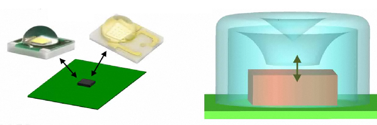
LED
Use an LED material device to simulate an LED.
- Specify the LED Thermal Resistance spec value (Theta) as Theta-JB on the Material Editor.
- If no value is available, assume a Theta-JB value of 10 C/W. Typical values are from 5-20 C/W.
- The value of Theta JC is seldom supplied for LED devices. Specify a value of 1000. This value ensures that the majority of the heat is conducted through the PCB instead of out the top of the device.
For more about LED material devices...
Printed Circuit Boards (PCB)
Printed circuit boards play an important role in many LED applications. They contain the electronics, but also are an important part of the thermal management within the device. In many applications, heat is dissipated directly from the LED to the PCB and then to the outer fixture casing.
For most applications, use the PCB material device to simulate the layers of a PCB. A simple alternative is the 12-layer-PCB solid material. The thermal conductivity values are pre-defined to represent a generic 12-layer PCB composed of FR4 with copper traces.
There are, however, a few special cases in which a more direct modeling approach is more appropriate:
Thermal Vias
Thermal vias are found in many LED applications, and are often critical for dissipating heat from the LED. There are three primary ways to simulate vias on a PCB:
- In the CAD model, divide the PCB so that a the region occupied by the vias is a separate volume within the PCB. In Autodesk® CFD, assign a higher conductivity to this region in the direction orthogonal to the board. This provides a conduction path through the board in the same direction as the vias would provide.
- Model the vias geometrically in the CAD tool. This approach is not generally recommended due to the geometric complexity of vias and the associated penalty in terms of analysis size and time.
- Ignore the vias. This approach produces a more conservative temperature distribution as it neglects the heat transfer provided by the vias directly from the LED through the board.
Metal Core PCB
Metal Core PCBs (MCPCB) are also found in many LED applications. There are a few ways to model them:
- Create multiple volumes in the CAD model to simulate the metal core and the dielectric layer.
- If a CTM or LED material is attached to the dielectric layer part, the material needs to include "PCB" in its name.
- The dielectric layer volume may be very thin relative to the metal core. In some models, this may cause meshing difficulties.
- Use a volume to model the metal core and a surface part to model the dielectric layer.
- Assign aluminum (or some other suitable material) to the metal core part. The material must have "PCB" in its name.
- To simulate the effect of both a dielectric layer and a copper foil, assign an equivalent thermal conductivity to the surface part.
- This method predicts the thermal spread better than the other methods.
- Create a single volume to represent the PCB in CAD.
- Assign a PCB material, and specify a single layer that is 100% metal. Note that this approach, while easier, is not as accurate as the others.
Heat Loading
- Assign a thermal load to each LED by specifying a volumetric heat generation boundary condition.
- The LED input power is the product of Voltage and current. Typically, 75% of the input power is dissipated as heat (the rest is light).
- A good way to account for heat dissipated from non-LED components is to assign the combined load to the PCB, and not model the individual parts.
- Apply a heat generation boundary condition that is 75% of the power supplied to the LED.