Printed Circuit Boards
Printed circuit boards (PCB) are used in a wide variety of electronics applications. Because PCBs play an important role in the temperature and heat flux distribution within a device, it is important to accurately represent their thermal characteristics accurately.
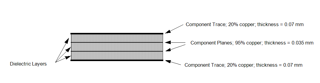
PCBs are typically constructed of multiple layers of copper foil and a dielectric material (a glass-reinforced polymer called FR4):
Example:
Total thickness = 1.6 mm
Because of the complexity of these components, it is often desirable to model them using simple geometry in conjunction with effective properties to simulate the heat transfer. Two conductivity values are needed: the normal conductivity (K-normal) and the in-plane conductivity (K-in-plane). These values are computed as shown:
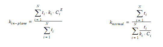
- N = the maximum number of layers
- k = layer conductivity
- t = thickness
- C = metal content
- E = coverage exponent
The Printed Circuit Board material type, is available to simulate the presence of a PCB within a simulation.
The PCB is represented as a simple geometric volume (even though physically PCBs can be quite complicated). The geometric physical specifications of the PCB such as the layer thickness and the amount of metal per layer are specified as material attributes, and the effective conductivities are then computed automatically and applied to the geometry throughout the analysis.
This material type provides a convenient way to include the thermal effects of a PCB in a simple, homogeneous geometry without having to include the geometric details of the various layers, traces, and planes:
Related Topics: