Prepare manufacturing data
Manufacturing data is generated by means of the CAM Processor. This processor uses Gerber RS274X files by default; it also supports Gerber X2 files for plotting, and Excellon files for drill data. These files are generated by Electronics, checked for accuracy as necessary, and then sent to the board manufacturer.
Manufacturers can provide a design rules (.DRU) file that details the standards they expect in board design. If used, a DRU file should be loaded before board layout, and especially before routing the traces.
Process overview
Preparing your manufacturing data is not a specific procedure, but varies according to the requirements of each board. A general overview is as follows:
On the circuit board document RULES DRC/ERC tab, click Design Rules Check (DRC)

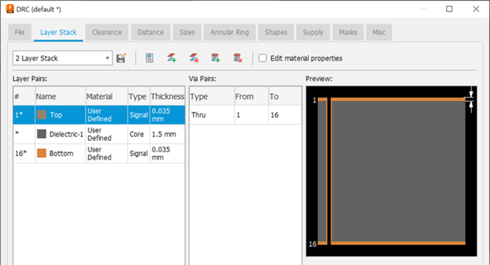
In the DRC dialog, check several tabs for accuracy of details such as Layers, Clearance, Distance, and Sizes.

Run MANUFACTURING > CAM Preview to check the board properties.

In CAM Preview, you see plated through-holes (PTH) for electrical connections, and non-plated through-holes (NPTH) for screws or other non-electrical uses. Note also the Drills tab for drill types and number.
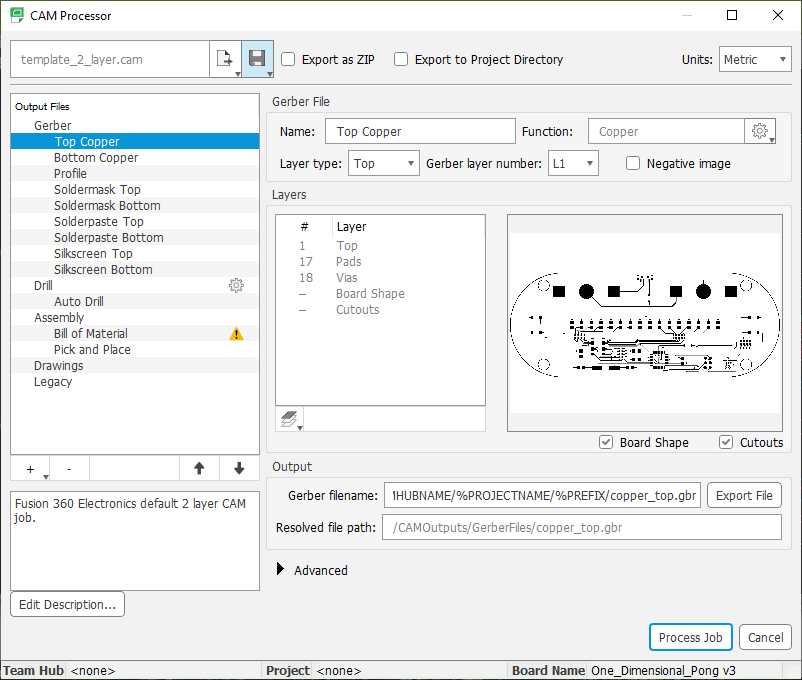
Optionally, run MANUFACTURING > CAM Processor to review the need for manual changes, such as adding layers, or deleting sections of the board.

Here you can also inspect the manufacturing output files. When finished, click Process Job to create the manufacturing files in a ZIP archive and specify a directory location for the files.
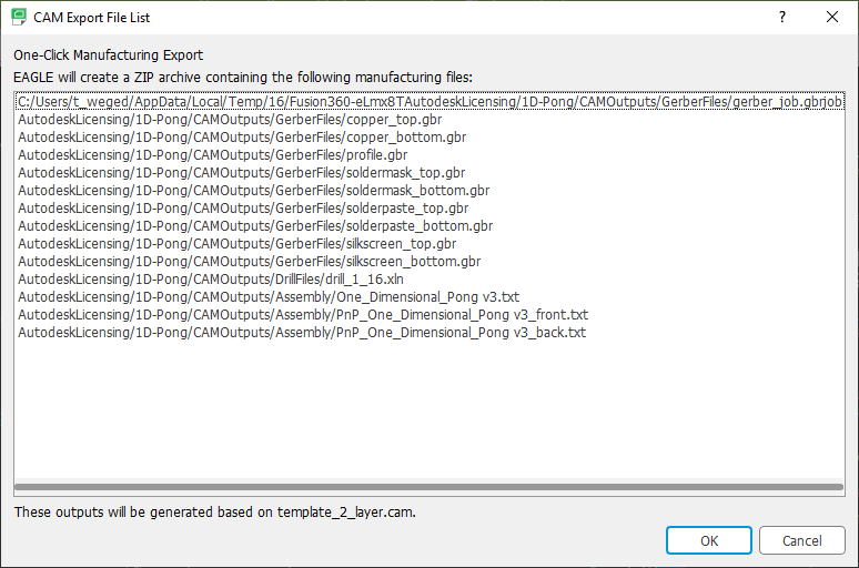
If all board details are correct, you can run MANUFACTURING > CAM Export as a one-click process to export the manufacturing files in a ZIP archive to a specified directory location.

Along the bottom of the dialog, you see that Electronics recognized this as a two-layer board and used an appropriate system template.
Additional details of the process are provided in the sections that follow.
On the DESIGN tab, LAYERS > Display is useful for reviewing the layers of a board, showing or hiding layers in the process.

Show layers 1 (Top), 17 (Pads), and 18 (Vias) for preview of the top layer; show layers 16 (Bottom), 17 (Pads), and 18 (Vias) for preview of the bottom layer.
Information panels such as Inspector are useful for reviewing and modifying components and their attributes. For example, you can select values or names of devices and change the font from proportional to vector or fixed.
When you process a job in CAM Processor, separate subfolders are created for Assembly (TXT), Drill (XLN), and Gerber (GBR) files. If you click Gerber in the file list, then hover the cursor over the Output type field on the right side, you see a detailed explanation of Gerber file structure.
The Soldermask layer creates the board color and protects the board, exposing spaces for vias and drills.
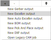
For Drill files, adding an Excellon output is an option, and you can specify the To/From layers. To do this, in the CAM Processor dialog, click the + sign at the bottom left of the Output Files panel, and click New Excellon output.

Prototype manufacture with a milling machine
With the help of User Language Programs (ULPs) you can generate outline data for milling a prototype board.
mill-outlines.ulp
A ULP that calculates outline and drill data is mill-outlines.ulp. It offers various configuration parameters. Simply start it with the RUN command in the Layout Editor.
This ULP exports for example CNC or HPGL formatted data or generates a Script file which can be imported into the layout again. The milling contours can be viewed, or even modified, if required. Generate the milling data with the CAM Processor and one of its devices, like Gerber, HPGL or PS.
Printing on a film
For boards of limited complexity, one can use a laser or ink jet printer and print on a transparent foil with the PRINT command. This method is used, for example, by hobbyists and results in a shorter fabrication time and a less expensive board fabrication process.
The layers that are displayed in the Layout Editor while printing will appear on the film. Check the options Black and Solid in the print dialog.
The drills of pads and vias are visible on the printout. This will allow an easy visual indication of where you have to drill manually on the board. Experience shows that the opening of a pad or a via should not be too big to allow for a good centering of the drill bit. This issue can be solved with the help of an User Language program, named drill-aid.ulp. Start it before printing, and let it draw a ring inside each pad and via in a separate layer. The inner diameter of this ring can be defined and is usually set to 0.3mm. Of course, you have to display this additional layer for printing on the film.
Data for pick-and-place machines and in-circuit testers
Electronics includes some ULPs that create data for various automatic placement machines and in-circuit testers that are typically used by PCB manufacturers.
The description of the ULP can be viewed at the bottom of the ULP dialog. It's also possible to edit the ULP file with a text editor. The description usually is written in the file header.
ULPs for pick-and-place data (selection)
| mount.ulp | Generates one file with coordinates of the centered part origins. |
| mountsmd.ulp | Centered origins for SMT devices; one file for top and one file for bottom side. |
ULPs for circuit tester (selection)
| dif40.ulp | DIF-4.0 format from Digitaltest |
| fabmaster.ulp | Fabmaster format FATF REV 11.1 |
| gencad.ulp | GenCAD format for Teradyne/GenRadin circuit tester |
| unidat.ulp | UNIDAT format |
| | |
| Execute the RUN command in the Layout Editor window to start the particular ULP. |
Documentation
Many documentation items can be generated with the aid of User Language programs. Note also the wide range of programs that are made available on our web server. The bom.ulp, the program for generating a bill of materials, has been used as a basis for lots of user-contributed ULPs.
Parts list
The parts list can be created by bom.ulp. Start it from the Schematic Editor, using the RUN command. The Bill Of Material window with the parts summary opens first.
It is possible to import additional information from a database file into the parts list (Load), or to create a new database with its own properties such as manufacturer, stores number, material number or price (New).
You can obtain further details about the current version of the ULP by clicking the help button.
A simple parts list can also be created from a board or schematic by means of the EXPORT command (Partlist option).
Drill plan
Printing a drill plan enables you to check the drill holes and their diameters. It shows an individual symbol for each diameter of hole, via, and pad used in your design. Electronics uses 19 different symbols: 18 of them are assigned to a certain diameter; one (Ø) appears, if no symbol has been defined for the diameter of this hole. The symbols appear in layer 44, Drills, at the positions where pads or vias are placed, and in layer 45, Holes, at the positions where holes are placed.
The relation between diameters and symbols is accessed by typing SET and pressing Enter in the CLI.
The buttons New, Change, Delete and Add can be used to create a new table, to modify certain entries, delete them or to add new ones. The Set button extracts all the hole diameters from the layout and automatically assigns them to a drill symbol number. The values of Diameter and Width determine the diameter and line thickness of the drill symbol on the screen and the printout.
Drill legend
Documenting the drill symbol assignment is quite simple with the help of a handy User Language program named drillegend-stack.ulp.
Now we start drill-legend.ulp. It draws a table with the proper drill symbol assignment and the drill symbols at their positions in the board in the newly generated layer 144. For printing, it can be helpful to display layer 20, BoardOutlines, additionally.
If you want to delete this all, simply use GROUP and DELETE in layer 144.