Set your Electronics preferences
Adjust your electronics preferences to design in ways that are efficient for you.
These preferences control default settings in Fusion Electronics. Any changes you make to the preferences are saved with your Autodesk ID and are loaded when you sign into Fusion on another machine.
Access the Preferences dialog
In the top-right corner, on the Application bar, click My Profile.
Select Preferences.
Check the following General settings:
- Default document preference is set to Electronics Design
- Domain Interest is set to Electronics. When Fusion starts the new document type is an Electronic Design document.
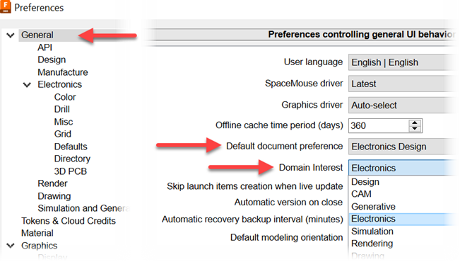
Expand the Electronics preferences list. Click on each item in the list to manage the preference.
About Electronics preferences
Electronics
Color
Drill
Specify your preferences for:
- Drill numbers and diameters
- Schematic symbol diameter and width
Misc
Set preferences for:
- Beep switches on/off the confirmation beep. Default: on.
- Check connects activates the package check while placing components in the schematic. Default: on.
- Optimizing enables the automatic removal of bends im straight lines. Default: on.
- Ratsnest processes polygons includes polygon contents when using the Ratsnest command. Default: on.
- Display pad names show pad names in 2D PCB or 3D PCB documents. Default: off.
- Display signal names on pads pads show signal names in 2D PCB or 3D PCB documents. Default: on.
- Display signal names on traces traces show signal names in 2D PCB or 3D PCB documents. Default: on.
- Display via lengths show the start and end layer names in the 2D PCB document. Default: off.
- Display drills show drill holes in pads and vias. Default: on.
- Auto end net and bus active net placement ends when placed on a pin or bus. Default: on.
- Auto set junction automatically adds a junction when ending a net on another net. Default: on.
- Auto set route width and drill uses the wire width and via length specified in the Design Rules or the net classes for traces. The value is automatically set when you click on a signal wire. Default: off. When off, the last specified value is used.
- Group command when in a 2D PCB document, nothing is selected, you can select a group as the default mouse action. Default: off.
- Minimum visible text size displays text greater than or equal to the minimum text size. Default: 3 pixels.
- Minimum visible grid size displays grid lines and dots whose screen proximity is greater than or equal to the minimum grid space. Default: 5 pixels.
- Catch factor defines the catch radius as a percentage of the active display window. Objects within the radius can be reached. Set the value to 0 to turn off this setting and reach objects that are placed farther away. Default: 5% of the active display window.
- Select factor defines the selection radius as a percentage of the active drawing window. Within this radius objects are selected. Default: 2%.
- Snap length defines the snap radius. Clicking when the cursor is within the radius distance from a pad or SMD connects the trace to the object.
- Xref label format defines the label text formatting used when displaying Xrefs.
- Xref part format defines the component name text formatting used when displaying Xrefs.
Grid
Preferences for displaying grids in schematic and board documents and how you want them to display.
Grid Schematic
- Display Grid: Select to display the grid when starting new schematic documents. Select grid units.
- Size: Defines the distance between grid points or line centers.
- Multiple:
- Alt: Defines the alternate grid. Activate this grid by holding down the Alt key. The grid is active as long as the key is depressed. The Alternate grid makes it possible to make finite adjustments in component position.
Grid 2D PCB
- Display Grid: Select to display the grid when starting new schematic documents. Select grid units.
- Size: Defines the distance between grid points or line centers.
- Multiple:
- Alt: Defines the alternate grid. Activate this grid by holding down the Alt key. The grid is active as long as the key is depressed. The Alternate grid makes it possible to make finite adjustments in component position.
Reset Grid
- Reset grid to default when opening schematic documents
- Reset grid to default when opening board documents
Defaults
Set the default value used for trace width, via diameter and drill size, PTH pad diameter and drill size, SMD pad size and roundness, polygon isolate and spacing, miter radius, text size, dimension line width, extension width, extension length, and extension offset.
Managing Default Preferences
You can add, delete, and restore default preference values for each of the default object types.
- Click the '+' (plus) icon to add a default value.
- Select a row and click the 'X' icon to delete the selected option.
- Click the reset button to restore the defaults for the associated option.
Directory
Set the paths used for libraries, design rules, ULP, scripts, CAM jobs, simulations, and SPICE models. The default paths are defined at installation.
3D PCB
Specifies whether or not to include the 3D PCB document when opening an electronics design.