The Compact Thermal Model material type allows the simulation of integrated circuits using a two resistor compact thermal model. Compact models provide a geometrically simple way to simulate the performance of electronic components using a resistor network.
This modeling method uses very simple geometry to represent a very complicated device. A more rigorous method uses the entire geometry of the device, and is often referred to as a “detailed model.” Detailed models typically produce the highest degree of accuracy, but due to their complexity, require a large mesh and hence require long analysis times.
The following chip configurations are supported by this type of modeling:
- BGA (ball grid array)
- PBGA (plastic ball grid array)
- TBGA (taped ball grid array)
- FC-BGA (flip chip ball grid array)
- QFP (quad flat pack)
- PQFP (plastic quad flat pack)
- NQFP (no-lead quad flat pack)
- SOIC/SOP (small-outline IC/ small-outline package)
Note that vertical chips such as the TO200 are not supported by this model. It is recommended to model such chips using a detailed model.
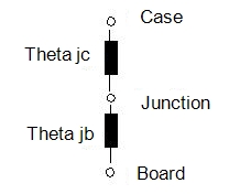
The typical two resistor compact thermal model consists of just three nodes: the junction, the case, and the board. The junction is also referred to as the die or the chip. The case is the top surface of the package, and is where a heat sink may be mounted to the package. The board node is a single point of contact between the board and the package. The nodes are connected by a thermal resistance between the case and junction (Theta jc), and a resistance between the junction and the board (Theta jb). The resistor network is shown:

In the two resistor compact model, heat transfer is only computed at the three nodes (case, junction, and board). The sides of a two resistor compact model are considered adiabatic. Only the case and board sides allow heat transfer to their surroundings. The case and board sides of the device are isothermal, and are modeled with a high conductivity in the in-plane direction.
Note that the two resistor compact model is a simplified representation of an actual device, and the literature indicates that they are typically accurate to about 10-30%. This model is a simplification, but one that is acceptable for many design-level “what if” analyses.
The resultant quantities of a two resistor compact model analysis are the temperatures at the board, junction, and case. In addition, the heat flux to the case and the board are provided.
Unlike a detailed component model, the two resistor compact model is modeled as a simple cuboid. The device must contact a PCB part, and a heat sink may be attached to the case side of the component.
In this example, the chip is positioned directly on the PCB:

Heat loading on a two resistor compact model is typically applied as a total heat generation boundary condition. Note that a transient heat generation condition can be applied, but because the specific heat and density of the component are not included in the material definition, a time-accurate solution will not be available.
Because the heat transfer computation is only performed on the three nodes of the network, a finite element mesh is not constructed through the device. The outside surfaces are meshed to provide connectivity between the two resistor device and the surrounding geometry.
Modeling Guidelines
CTM materials must contact a part that is assigned a fluid material. Autodesk Simulation CFD does not support CTM modules completely embedded in a solid object.
A CTM must only contact one PCB material (or a solid with "PCB" in its name). One common situation is to sandwich the CTM between two PCB materials. Another is for the CTM to straddle two adjacent PCB materials. Neither of these configurations is supported. The CTM must contact one and only one PCB.
One way to fix this is to modify the model configuration in the originating CAD tool. Move the CTM so that it touches only a single PCB part. Another approach is to modify the material definition of one of the PCB parts within Autodesk Simulation CFD. Either change the definition of one of the parts to a solid or assign a different solid material that does not include "PCB" in its name.
A CTM cannot contact a PCB material that is suppressed. A suppressed part cannot contact the board or case surfaces of the CTM.
Check the Material branch (of the Design Study bar) to ensure that the PCB part is not suppressed. Suppressed parts are displayed with a line through their name. To unsuppress the part, right click on it, and click Resume. Note that the mesh will have to be defined again.
Data Extraction and Visualization
For visualization purposes, the device is divided into two regions--the junction and the case. Each region of the component has its own temperature which is governed by the resistance values and the surrounding conditions. A single rectangular element comprises each layer, and is shown:

For every two resistor component, the following data is available:
- Board Temperature
- Junction Temperature
- Case Temperature
- Heat flux between the junction and the board (board-side heat flux)
- Heat flux between the junction and the case (case-side heat flux)
Results are viewed using these methods:
- In the Results task, click the Global icon. Hover your mouse over the desired chip. A window will appear listing the results data.
- Open the Component Thermal Summary from Review_Component Thermal Summary.
Related Topics