To Assign a Compact Thermal Material
- Open the Material quick edit dialog. There are several methods:
- Left click on the part, and click the Edit icon on the context toolbar.
- Right click on the part, and click Edit...
- Right click on the part name under the Materials branch of the Design Study bar, and click Edit....
- Click Edit in the Materials context panel.
- Select one or more parts.
- Select the database from the Material DB Name menu.
- Select Compact Thermal Model from the Type menu.
- Select the material from the Name menu.
- Click Apply.
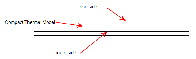
The compact thermal model must contact either a PCB material or a solid material with “PCB” in its name. ("PCB" must be in English.) From this, the orientation of the device is determined automatically.
The side of the component touching the PCB material is the board side, and the board node is at the center of the board surface of the component. The opposite side is the case side.
Additional Guidelines:
CTM materials must contact a part that is assigned a fluid material. Autodesk Simulation CFD does not support CTM modules completely embedded in a solid object.
A CTM must only contact one PCB material (or a solid with "PCB" in its name). One common situation is to sandwich the CTM between two PCB materials. Another is for the CTM to straddle two adjacent PCB materials. Neither of these configurations is supported. The CTM must contact one and only one PCB.
One way to fix this is to modify the model configuration in the originating CAD tool. Move the CTM so that it touches only a single PCB part. Another approach is to modify the material definition of one of the PCB parts within Autodesk Simulation CFD. Either change the definition of one of the parts to a solid or assign a different solid material that does not include "PCB" in its name.
A CTM cannot contact a PCB material that is suppressed. A suppressed part cannot contact the board or case surfaces of the CTM.
Check the Material branch (of the Design Study bar) to ensure that the PCB part is not suppressed. Suppressed parts are displayed with a line through their name. To unsuppress the part, right click on it, and click Resume. Note that the mesh will have to be defined again.
To Create a Compact Thermal Material
Only two parameters are required to define a two resistor Compact Thermal Model on the Material Editor:
- Theta JB: the resistance between the junction and the board
- Theta JC: the resistance between the junction and the case
- To open the Material Editor, click Material Editor on the Materials context panel.
- Click the List button.
- Right click on a custom database, and select New material. Select Compact Thermal Model. Specify a Name.
- Click either the Theta JB or Theta JC button.
- Enter a value and appropriate units. (Note that the only available variation method is Constant.)
- Optionally, click Save.
- Click OK. The new material is available when the Materials quick edit dialog is opened.
Data Extraction and Visualization
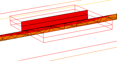
For visualization purposes, the device is divided into two regions--the junction and the case. Each region of the component has its own temperature which is governed by the resistance values and the surrounding conditions. A single rectangular element comprises each layer, and is shown:
For every two resistor component, the following data is available:
- Board Temperature
- Junction Temperature
- Case Temperature
- Heat flux between the junction and the board (board-side heat flux)
- Heat flux between the junction and the case (case-side heat flux)
Results are viewed using these methods:
- In the Results task, click the Global icon. Hover your mouse over the desired chip. A window will appear listing the results data.
- Open the Component Thermal Summary from Review_Component Thermal Summary.
Related Topics