Create the PCB Material
In this step, we create a Printed Circuit Board material.
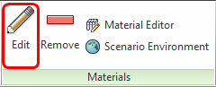
To open the Material quick edit dialog, click Edit from the Materials context menu:
Change the Type to Printed Circuit Boards.
On the Material line, click Edit...
Enter the name Board in the Name field.
Select My Materials from the Save to database menu.
Click the Total PCB Thickness button.
Value = 1.6; Units = millimeter
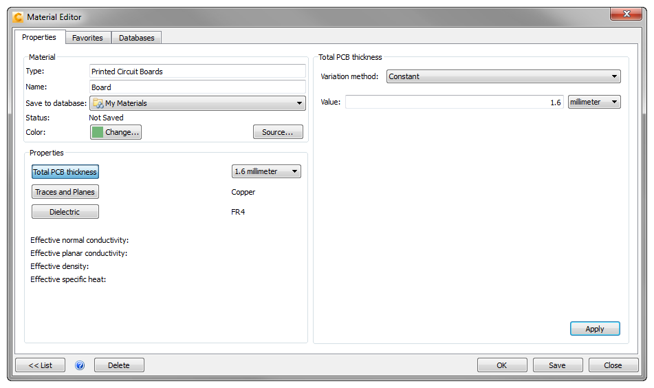
Click Apply.
Click the Traces and Planes button
Material = Copper
Layer 1: Thickness = 0.07; %metal= 20
Layer 2: Thickness = 0.035; %metal = 95
Layer 3: Thickness = 0.07; %metal = 20
Layer 4: Thickness = 0.035; %metal = 95
Delete all data points on rows after Layer 4.
Coverage Exponent = 2
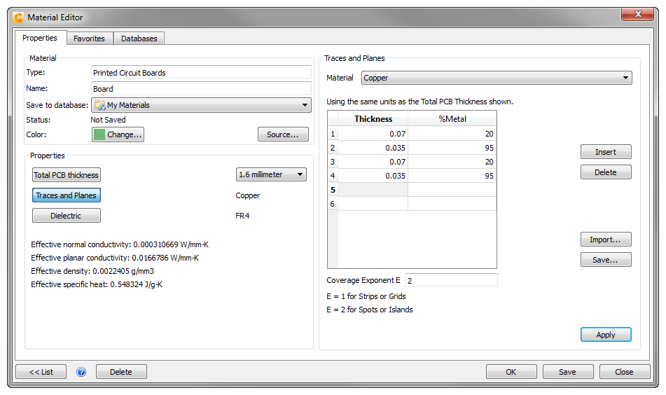
Click Apply.
Click the Dielectric button.
Click Save.
Click OK.
For more about PCB Material Creation