Electronics drawings
Electronics drawings are part of the manufacturing dataset, used by technicians and engineers to diagnose boards and verify proper construction. In a volume production scenario, they are generated for all designs irrespective of layer count.
The following image shows (1) the electronics drawing browser node structure and (2) electronics drawings and related views and tables supported across multiple drawing sheets.
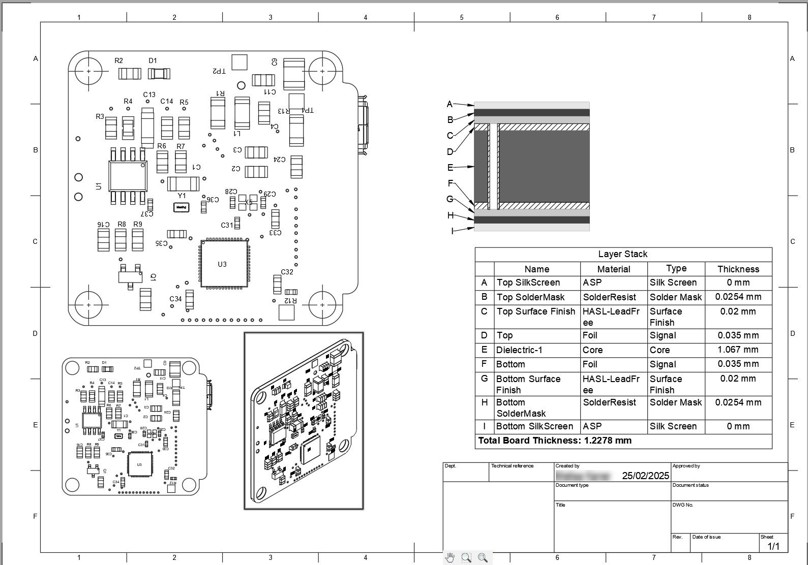
Layer stacks
Add a Layer Stack Table alongside a Layer Stack Diagram to see detailed information about each layer, such as material, thickness, type, and any special attribute. Together, they enable thorough verification of the PCB design, ensuring that it meets the required standards and performance criteria before production begins. They also let everyone understand the physical structure and specifications of the PCB. You can place layer stacks for multiple PCBs in a mechanical assembly alongside each other on a single sheet or across multiple sheets for more detail about the boards within the entire assembly.
Silkscreen
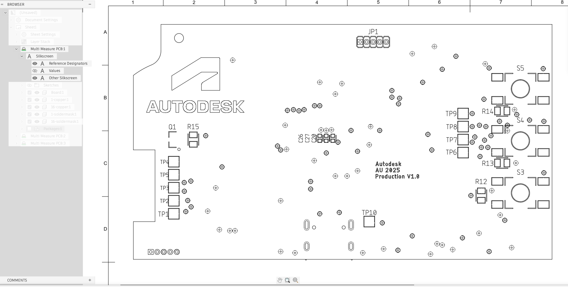
In the Browser, you can view silkscreen objects such as logos, symbols, values, and reference designators. Select the silkscreen or documentation layers from the 2D PCB layer set selection to include or exclude them during electronics drawing creation.
TopSilkscreen and BottomSilkscreen editable layer sets to control their visibility in the Model Views in Drawings,- When added to these editable layer sets,
NamesTopandNamesBottomwill appear on the Reference Designator node in the Drawings Browser. ValuesTopandValuesBottomwill appear on the Values node.- All other layers in the silkscreen layer sets will appear on the Other Silkscreen node.
 |
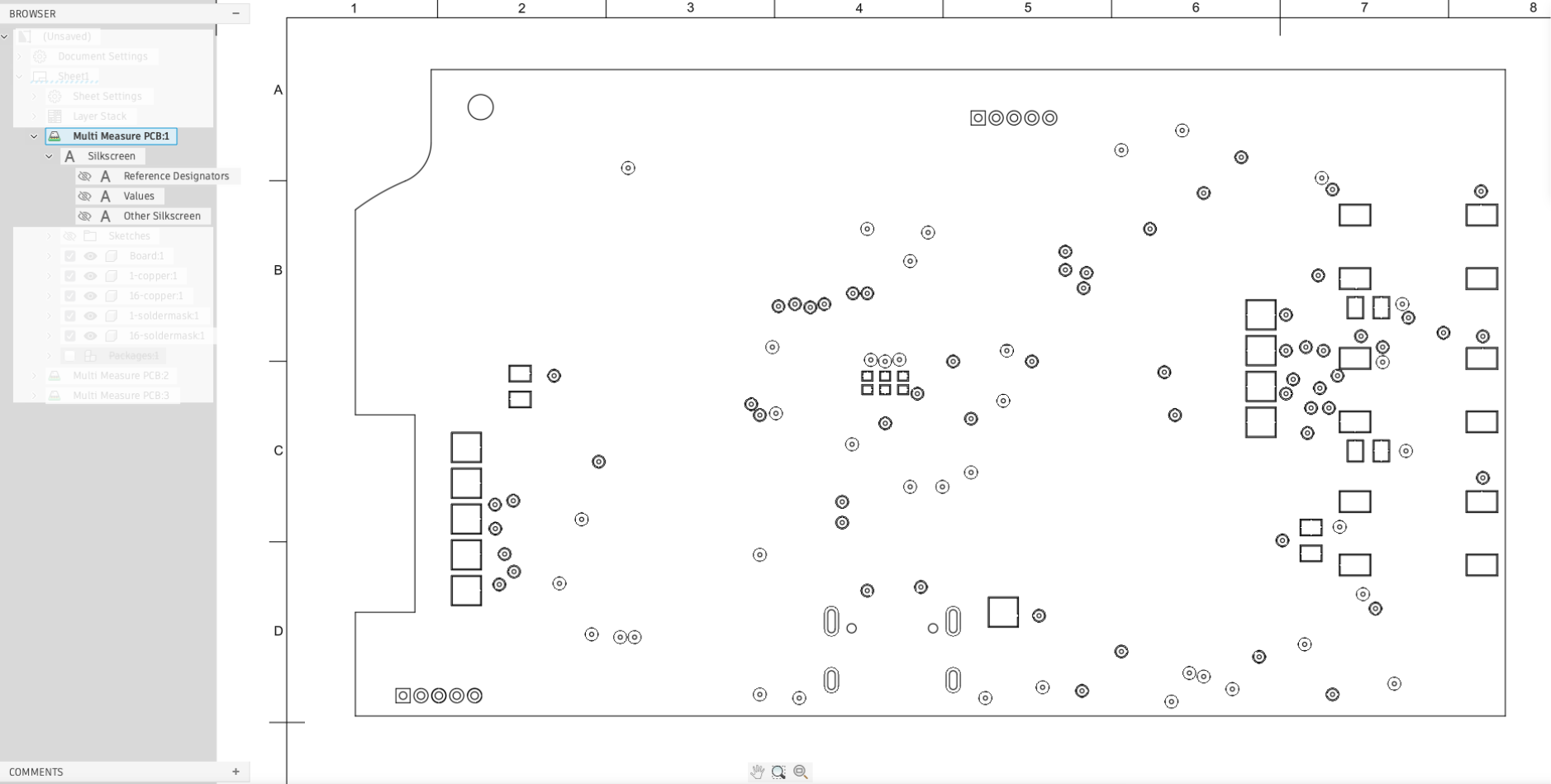 |
| Reference designators and other silkscreen objects visible | All silkscreen objects hidden |