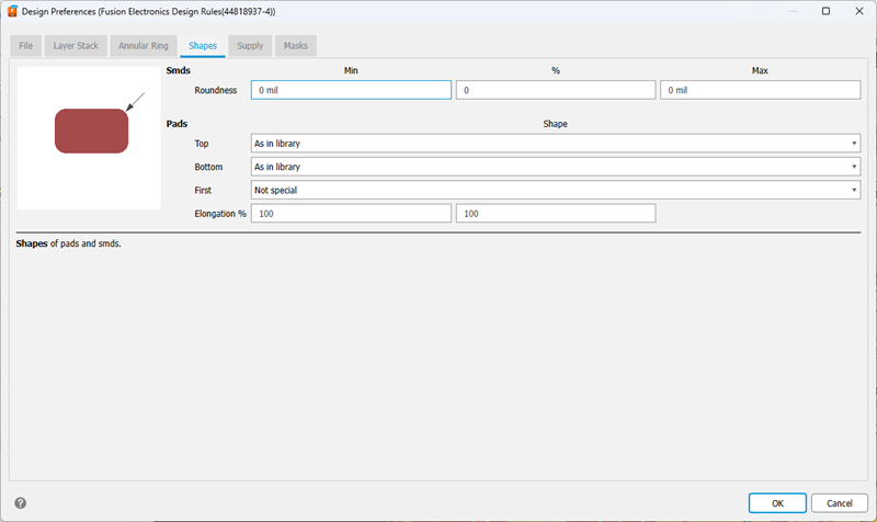
Shapes
SMDs
A rounding factor can be specified here for SMD pads. The value can be between 0% (no rounding) and 100% (maximum rounding).
Pads
This is where the form of the pads is specified. It is possible to give different settings for the top and bottom layers.
The As in library option adopts the form defined in the Package Editor. Click Apply, shows the change immediately in the Layout Editor.
Pads and Vias within inner layers are always round, no matter what they are in Top or Bottom layer. The diameter is determined by the annular ring settings.
Provided a pad was given the First flag in the library one can specify a certain shape for all those pads in the layout.
Elongation defines the aspect ratio of length to width of Long and Offset pads (see image). The value is given in percent. Click with the mouse into the box Long or Offset and the image on the left shows the corresponding calculation rule.
100% is equivalent to an aspect ratio of 2:1. 0% results in a normal octagon pad with an aspect ratio of 1:1. The maximum is 200% (ratio 4:1).

Notes on the display in the Layout Editor
If pads or vias have different shapes on different layers, the shapes of the currently visible (activated with DISPLAY) signal layers are displayed on top of each other.
By default, vias and pads share color. To show which layers vias connect to, go to Preferences > Electronics > Color and check Show Vias and Pads in respective copper layer colors.
This also applies to printouts made with PRINT.