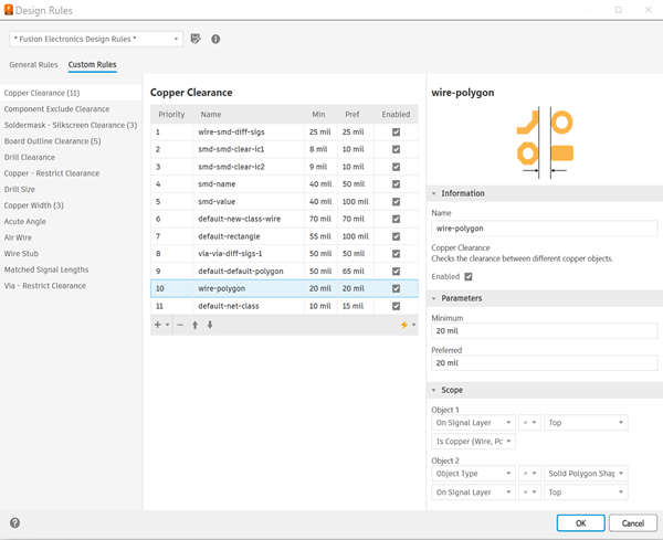
Design rules
Fusion uses Design Rules to define the requirements of a design. These rules create an instruction set for Fusion to follow, so the PCB meets the design standards. It checks the PCB board against these design rules but ignores electrically irrelevant objects like rectangles, circles, and texts, for clearance errors unless they are on Signal Layers. To verify your board adheres to the design rules, run the Design Rules Check (DRC) routine after designing your board. This will identify any errors.
Fusion applies design rules based on their priorities, checking the highest priority first during tasks like manual routing. This includes checking for clearance, copper width, or VIA drill size. Set rule priorities to check the strictest scopes first, followed by less strict ones.
Create PCB designs that meet stringent manufacturing requirements with a defined set of design rules. Set up these rules at the start of the design process so you can focus on the design without worrying about manufacturability. Adjust the rules in the Design Rules as needed. You can save the customized rules as a new Fusion Electronic Design Rule (EDRU) file with a new name.

The UNDO/REDO function captures changes to the Design Rules.
Design rule scopes in interactive workflows
The following interactive workflows use all design rules, including custom ones:
Copper Pouring:
- Clearance calculation: Uses the best applicable clearance rule preferred value.
Manual Route:
- Clearance calculation: Uses the best applicable clearance rule preferred value.
- Copper width: Uses the best applicable copper width rule preferred value.
- VIA drill size: Uses the best applicable drill size rule preferred value.
Multi Route:
- Clearance calculation: Uses the best applicable clearance rule preferred value.
Differential-Pair Route:
- Clearance calculation: Uses the best applicable clearance rule preferred value.
Note: The best applicable rule is the first rule where objects match the Object 1 (all rules) and Object 2 scopes (binary rules only). For same signal copper clearance rules, the Both Objects scope must also match.
When you use autocomplete, Quick Route, Multi Route, Differential-Pair Route and Meander can only use the following signal-based rule scopes:
- In Net Classes
- In Signal
- Is Signal
- In Diff Pair
- In Named Group