
Electronics Design document
The Electronics design document is the primary (umbrella) document that manages the synchronization between the schematic, 2D PCB, and 3D PCB documents. As you create the schematic, and board documents, by default they are arranged in separate tabs of a single Fusion window. You can undock these document tabs if you prefer to work with schematics, board designs, and libraries in separate side-by-side windows.
Within the design document, as you create the schematic, 2D PCB and 3D PCB documents, they are listed in the left panel, and appear as thumbnails in the right.
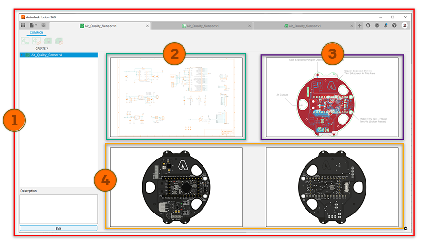
Figure 1: (1) Electronics design document showing (2) Schematic, (3) 2D PCB, and (4) 3D PCB documents listed on the left and as thumbnails on the right.
The Design document is the primary (umbrella) document that manages the synchronization between the three other documents. New designs always start with the design and schematic documents.
The Schematic document is where you document the logic and functionality of the design by adding symbols representing the various board components and their connections. Schematic documents can contain up to 999 sheets, as needed, to document the design logic. The schematic and 2D PCB documents are automatically kept consistent by the Electronics Design Workspace.
The 2D PCB document is where you layout the components in relation to one another. You can generate the associated circuit board at any time with a single mouse click. A 2D PCB document is opened and all of the schematic components are placed next to the empty board. Components have thin yellow lines (sometimes called air wires) representing unrouted, point-to-point connections between components. You can define or import a board shape and then use the 2D PCB tools to locate components on the board.
The 3D PCB document is 3D model generated from the 2D PCB data. The 2D and 3D PCB documents are generated from the schematic and include components from the libraries you reference. The component 3D models may be included in the library along with the logical symbol and component footprint, this collection is referred to as a 3D package. If a component doesn't have an associated 3D model, a placeholder shape (rectangle) is substituted when generating the 3D document. You can map 3D models to components in the 2D PCB workspace.