
2D PCB document
You can create a 2D printed circuit board (PCB) at any time after starting work on the associated schematic.
Initially, an empty board is generated, with the components from the schematic placed alongside, and joined together by white lines known as airwires. You drag the components onto the board, as shown below:
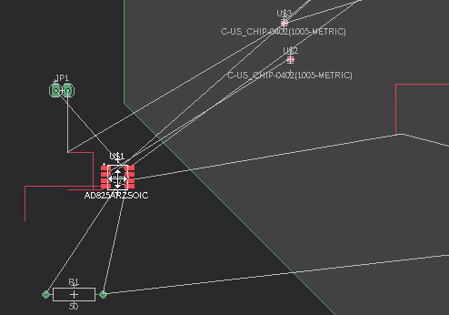
As you move components on the board, an algorithm known as 'ratsnest' optimizes the airwire paths to be as direct as possible between the various connection points.
The placement grid for components is set to 50 mil (1.27 mm) by default. If you prefer a different placement grid, click the Grid icon ![]() at the bottom of the window.
at the bottom of the window.
The board is linked to the schematic by the Forward&Back Annotation engine, provided that both files are open. Alterations made in one file are automatically carried out in the other.
After generating a board from your schematic, if you continue placing components in the schematic, the referring packages in the board are placed in the current grid setting of the Layout Editor.
If the 2D PCB is not open when you edit the schematic, Forward&Back Annotation can't function and the 2D PCB and schematic documents will be out-of-sync. You can manually resolve the differences with the aid of the error messages provided by the Electrical Rule Check (ERC).
Video: How to create a printed circuit board layout
Key concepts:
- Defining a shape
- Placing components
- Routing wires
Length: 4:33