My Learning - Electronics workspace
Here are the My Learning campaigns for the Electronics workspace.
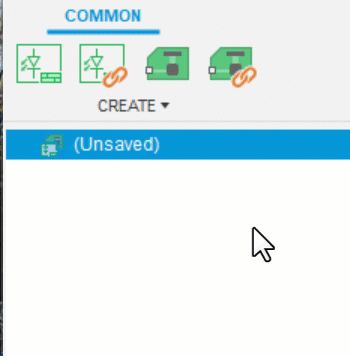
Electronics > Common > New Schematic
Create a new schematic
The schematic design serves as a logical representation of the electronic circuit board. It defines the components that are being used for the design and how are they connected.
Electronics > Common > Reference to a Schematic Document
Reference a schematic
In a new electronics design, use the Reference to a Schematic Document tool to reference Schematics from other designs.
Electronics > Common > Create PCB Board
Create a new PCB
The PCB editor is used to lay out the circuit board using the assets that were placed in the schematic. Component footprints are automatically included in the PCB editor. Changes between the schematic and PCB documents sync automatically.
Electronics > Common > Reference PCB
Reference a PCB
In a new electronics design, use the Reference to a PCB Document tool to reference a PC board created in another design into the current design. Click Common > Create > Reference to a PCB Document.
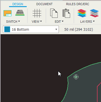
Electronics > PCB > Move Components
Move Components
Once Schematic is switched to PCB design all components are on the left side of the board.
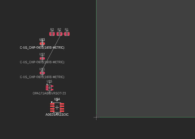
Move the components to the board by clicking and holding the component and then dragging it into position.
Electronics > PCB > Manual Routing
Manual Routing
Route allows the nets to be converted into tracks.
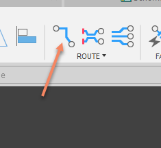
Route offers two different modes: Walkaround obstacles (default) and Ignore obstacles. These modes can be selected in the parameter toolbar of the Route tool. The following image is an example of a manual route.
Electronics > PCB > Board Shape
Board Shape
When creating a board layout a default board boundary is put in place for you. However, you can either move the current boundary or draw a new one. For drawing a new one there are four options:
- Outline Polyline
- Outline Spline
- Outline Arc
- Outline Circle
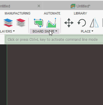
Once new board layout is drawn delete the initial layout.
Electronics > PCB > Via
Via
A Via has two pads in corresponding positions on different layers of the board, that are electrically connected by a hole through the board. To create a Via, click Design > Fanout > Via. Note: Once new board layout is drawn delete the initial layout.
Electronics > PCB > DRC
DRC
The Design Rules Command is used to set various design and rules standards for when you are laying out your PCB board.
You can control:
- Wire Size
- Board layers
- Clearance for Pads/Vias
- Masks
- And so on
To access the DRC dialog, click Rules DRC/ERC > DRC > DRC.
Electronics > PCB > 3D PCB
3D PCB
Once your board is laid out and the routes, vias, and everything else is in place, it is time to view your creation in 3D. Click Design > Switch > Push to 3D PCB.
Electronics > Schematic > Add Frame
Add Frame
A Frame in the Schematic workspace represents a drawing border for the drawing. To add a frame to your schematic, set the layer to use for the frame, then in the CLI enter "frame". In the canvas, draw a frame. Right-click the frame in the canvas and click Properties to manage the sheet size.
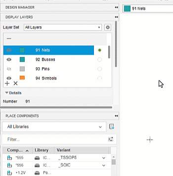
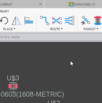
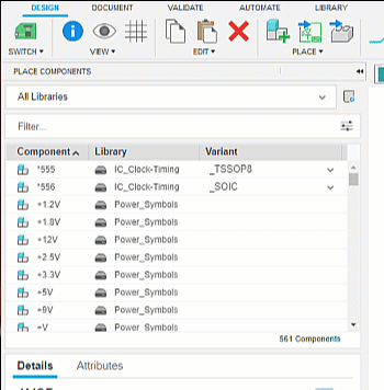
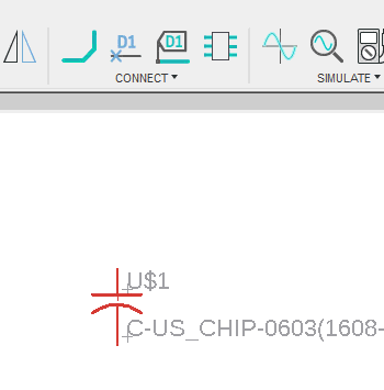
Electronics > Schematic > Place Component
Place Component
Displays the Place Components panel which provides access to component libraries so you can add components to your current project. To add a component to your Schematic, double-click a component, drag and drop a component, or select a component and press Enter. View details and attributes in the lower section of the panel.
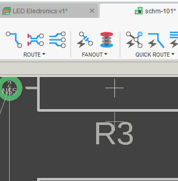
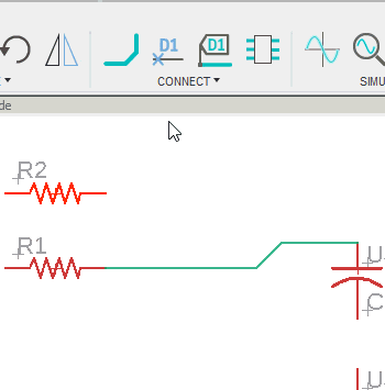
Electronics > Schematic > Trace/Net
Trace/Net
Net is what will be used to manually draw the connections from component to component. To add Nets to your Schematic, click Design > Connect > Net. Select points to draw in the lines between components.
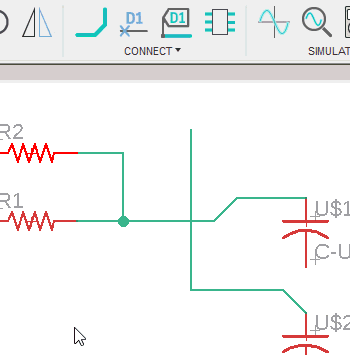
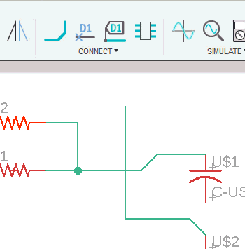
Electronics > Schematic > Junction
Junction
There are two ways in Fusion Electronics to create junction points.
- Create when drawing out Nets
- Create with Junction
To create using the Net tool, start off on a component and end the net on another line.
To create using the Junction tool, click Design > Connect > Junction. Then select the point to place the junction, then select the line to connect.
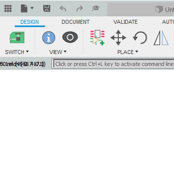
Electronics > Schematic > Stop Commands
Stop Commands
When working with Fusion Electronics tools, they don't always stop once done using them. To stop them completely, you must click the Stop Command button.
Electronics > Schematic > Line Labels
Line Labels
To identify the nets as you build out the schematic, it is helpful to place labels on the lines.
Electronics > Schematic > Switch to Board
Switch to PCB document
Use to move between the schematic and the pcb documents. An alternate to using document tabs.
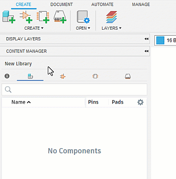
Electronics > Common > Create Electronics Library
Create Electronics Library
Use libraries to organize and maintain the objects used in board layouts. Click File > New Electronics Library.
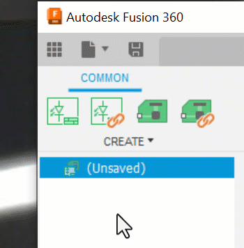
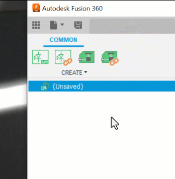
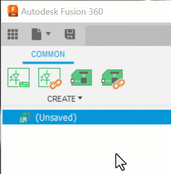
Electronics Library > New Component, Symbol, or Footprint
New Component, Symbol, or Footprint
Create or import components, symbols, or footprints to build an electronics library. In the Create panel, click New Component, New Symbol, or New Footprint.