
Edit a 3D PCB inside its enclosure
From an Electronics Design
Open your 2D circuit board design that you want to convert into a 3D PCB.
Click Switch > Push to 3D PCB.
Optionally, on the 3D PCB toolbar, click Modify > Move Component to adjust the position of components on the board
Optionally, on the 3D PCB toolbar, click Modify > Flip Component to flip a component to the opposite side of the board.
Click PCB > Push to 2D PCB to keep both documents synchronized.
Note: If the 3D board was created independently, you can link the 3D design to a 2D PCB, if a suitable design exists.
From a Mechanical Design
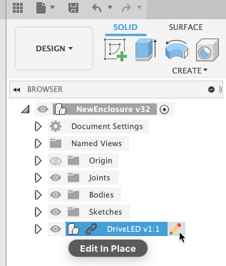
Activate Edit In Place for the 3D board by clicking the pencil icon beside the board drawing name in the browser.
On the Edit In Place menu at the top of the drawing window, select Associative.
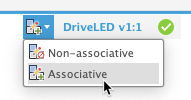
This setting is required to support automated updates between 3D and 2D circuit boards when using Edit In Place.
From the 3D PCB panel, you can use the Flip tool to move components to the other side of the board and the Move tool to better align components with openings in the enclosure.
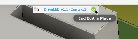
Exit the Edit In Place mode by clicking the green check mark on the Edit In Place menu at the top of the drawing window. Save the Design workspace for the board and enclosure.
Click the 3D PCB drawing tab, then reopen it from the Data Panel to get the Edit In Place updates from the Design workspace for the board and enclosure.