Multilayer boards
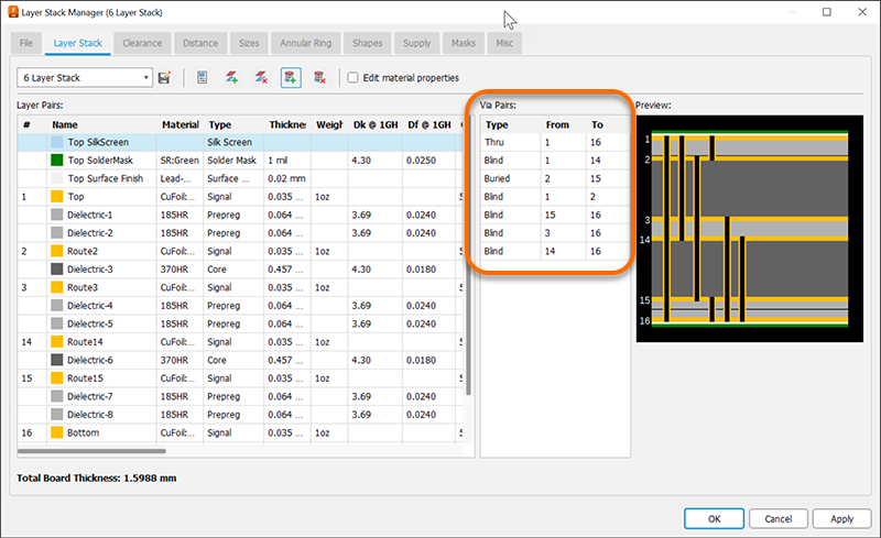
Usually you create multilayer routing when you are working with small, dense boards, such as for robotics. With these types of boards, instead of just using “Through” vias that go all the way through the board, you create vias that optimize the amount of space used:
- Blind vias: pass from an outer layer to an inner layer
- Buried vias: pass from an inner layer to another inner layer
Circuit boards are manufactured from inner to outer layers. The more inner layers you route to, the more complex your board will be. Boards with more than two layers tend to be more expensive to make, and can be more difficult to troubleshoot.
Before routing your layout, you should be aware of:
- The number of signal layers to use
- Whether vias should go through all layers
- If, due to the complexity of the layout, you need to work with blind, buried or micro vias.
If you expect to use blind, buried, or micro vias, Autodesk recommends contacting your board manufacturer to discuss the possible structure of the board and the costs to be expected.
Inner layer
Inner layers are used the same way as outer layers (Top and Bottom). They can be filled with copper areas (polygons) as well. Before using inner layers you must define them in the Layer Stack Manager. (Design > Layers > Layer Stack Manager).
Supply layers with polygons and more than one signal
You can use the POLYGON command to fill areas of the board with a particular signal (such as ground). The associated pads are then automatically connected using Thermal symbols. Specify the isolate value for the Thermal symbols in Design Rules (Rules DRC/ERC > DRC > Supply). The width of the connecting bridge depends on the line thickness with which the polygon is drawn. You can also specify whether or not vias are to be connected through Thermals. The minimum clearances from objects carrying other signals specified in Design Rules are maintained (Clearance and Distance tabs). Changes are shown in the layout when the polygon is next computed (RATSNEST command).
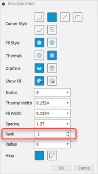
This way you can create layers in which several areas are filled with different signals. You can assign different ranks (priorities) for the polygons. The rank property determines which polygon is subtracted from others if they overlap (Design > Polygon > Polygon Pour ![]() ).
).

- Rank = 1: The highest priority in the layout. Nothing will be subtracted from this type of polygon.
- Rank = 6: The lowest priority in the layout. Polygons with the same rank are compared by the DRC.
Restricted areas for polygons
For creating non-copper areas for polygons in inner layers, use a cutout polygon (Design > Polygon > Polygon Cutout ![]() ). This type of polygon, with the fill style cutout, defines an area which is subtracted from all other signal polygons in this layer. You can draw a cutout polygon with any wire width, even 0. Compared to signal polygons, a cutout polygon does not create large amounts of manufacturing data. Signal polygons respect the wire width of the cutout polygon. The dotted line of the contour is always visible, but is not a part of manufacturing data.
). This type of polygon, with the fill style cutout, defines an area which is subtracted from all other signal polygons in this layer. You can draw a cutout polygon with any wire width, even 0. Compared to signal polygons, a cutout polygon does not create large amounts of manufacturing data. Signal polygons respect the wire width of the cutout polygon. The dotted line of the contour is always visible, but is not a part of manufacturing data.
Multilayer boards with through-hole vias
Use this type when possible. Vias go through all signal layers and are drilled at the end of the production process. Production costs are moderate.
Layer setup
Set layer composition and number of signal layers in the Layer Stack Manager.
For through vias the setup is very simple. No considerations about thickness of copper and isolation layers are necessary.

Multilayer with blind and buried vias
In high density boards it is often necessary to use Blind and Buried vias. These kinds of vias don't connect all layers, but rather are only reachable from a certain number of layers. How these layers are connected depends on the manufacturing process of the board which has to be determined in the Layer setup in the Design Rules.
Contact your board house before starting your work. Check what kind of layer setup is suitable for your purpose and what the manufacturing costs are.
Hints for working with blind, buried, and micro vias
VIA command
Depending on Layer setup, vias can have different lengths. The parameter toolbar of the VIA command shows all available lengths in the Layer box. When routing manually (ROUTE command) Electronics takes the shortest possible via length in order to change layers. It is also possible that vias at the same position are elongated.
To change the length of a via, you can use the CHANGE VIA command. Select the value from the menu and click the via with the left mouse button.
Alternatively use the command line:
CHANGE VIA 2-15
Click the via to change the length from layer 2 to 15. If the given via length is not defined in the Layer setup it will be elongated to the next possible length or, if this is not possible, an error message will be generated.
The command:
VIA 'GND' 1-4 (1.05 2)
places a via that belongs to the signal GND and reaches from layer 1 to 4 at position (1.05 2).
ROUTE command
If you want to change the layer while laying out the board, Electronics always uses the shortest possible via (CHANGE LAYER command; also in Follow-me mode). It is also possible that a via at the same position will be elongated automatically.
Micro via − a special case of blind via
In contrast to blind vias that can reach several layers deep into the board the micro via connects an outer layer with the next inner layer. The drill diameter of a micro via is relatively small. The usual values are about 0.1 to 0.05 mm.
For manufacturing reasons micro vias, as blind vias, have to follow a certain aspect ratio of depth to drill diameter. This ratio defines the maximum via depth for a certain drill diameter. The proper value can be learned from your board house.
Set this value under Design Rules, Sizes tab, Min. Blind Via Ratio. If the board house requires the ratio to be 1:0.5, you must enter 0.5 for Min. Blind Via Ratio.
Additionally the Design Rule Check verifies the minimum drill diameter for Micro vias given in Min. MicroVia. If this value is higher than the value for Minimum Drill (default), micro vias won't be checked.
The diameter of micro vias is set in the Annular ring tab of Design Rules.
If you change the layer from an outer to the next inner one while you are routing a track out of a SMD, Electronics automatically places a micro via, provided Design Rules allow it.