
Sync changes between 3D PCB and 2D PCB
When trying to add a 3D PCB into an enclosure, you may find that components and traces need to be moved. For example, when this board was moved into its enclosure, three design errors were identified. The top error is a trace that runs too close to a hole in the board. The two errors on the right side are traces and components that are too close to the edge of the board.
These issues can all be fixed by re-routing traces and moving components in the 2D design.
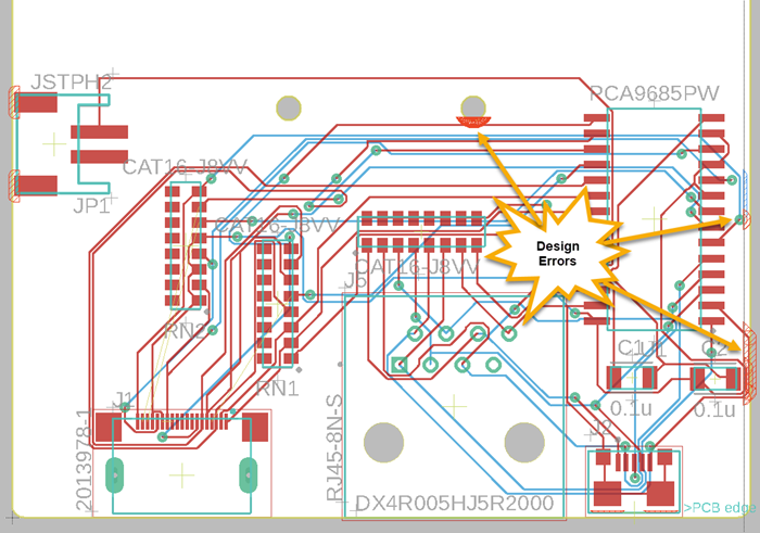
Figure 1. Design errors in the 3D board.